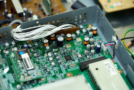
Masters & Young provides specialised high-speed printed circuit board (PCB) design and manufacturing for organisations in defence, aerospace, telecommunications, medical, and industrial fields. Drawing on more than 25 years of engineering experience, our Brisbane-based team delivers high-frequency PCB solutions built for accuracy, reliability, and compliance in applications where fast signal performance is critical.
When your product relies on fast signals, dense layouts or performance-sensitive electronics, PCB design decisions can directly affect signal integrity, timing, EMI control and long-term reliability. High-speed PCB design helps ensure the board is planned around controlled impedance, stack-up, routing, return paths, material selection and manufacturability from the start.
Masters & Young supports Australian electronics projects with high-speed PCB design, prototyping, assembly, testing and manufacturing from our Brisbane facility. Our team can assist with board architecture, multilayer stack-up planning, signal integrity considerations, design for manufacturability, component sourcing, testing requirements and production planning.
High-speed PCBs provide more than just faster data transfer. They deliver a range of performance and reliability advantages that are critical in advanced systems, including:
Masters & Young offers end-to-end support for high-speed PCB projects, combining advanced design techniques with rigorous testing and manufacturing. Our services include:
By applying our Define, Design, Deliver methodology, we create high-speed PCB solutions that achieve performance targets while remaining manufacturable at scale.
Choosing Masters & Young for your high-speed PCB design means working with a partner trusted by leading organisations across Australia. Our advantages include:
Masters & Young is trusted by defence and aerospace, mining, medical, and industrial clients for dependable high-speed PCB design and manufacturing. If your project requires precise, compliant, and high-performance boards, our Brisbane-based team is ready to assist. Contact us online or call (07) 3208 6555 today to discuss your high-speed PCB design requirements.
High-speed PCBs are widely used in telecommunications, aerospace, defence, medical imaging, radar, and high-performance computing systems.
Yes, they can be more expensive due to advanced design techniques, tighter tolerances, and specialised manufacturing processes.
When designed correctly, high-speed PCBs provide stable, accurate performance even in demanding, mission-critical environments.
Not always, but multilayer design stack-ups are common to improve signal integrity, reduce interference, and support complex circuits.
Yes. We provide prototyping services to validate signal integrity and performance before moving into production.
Yes. Our high-speed PCB layouts are created with EMC in mind, and we support clients through the compliance process to achieve first-pass success.