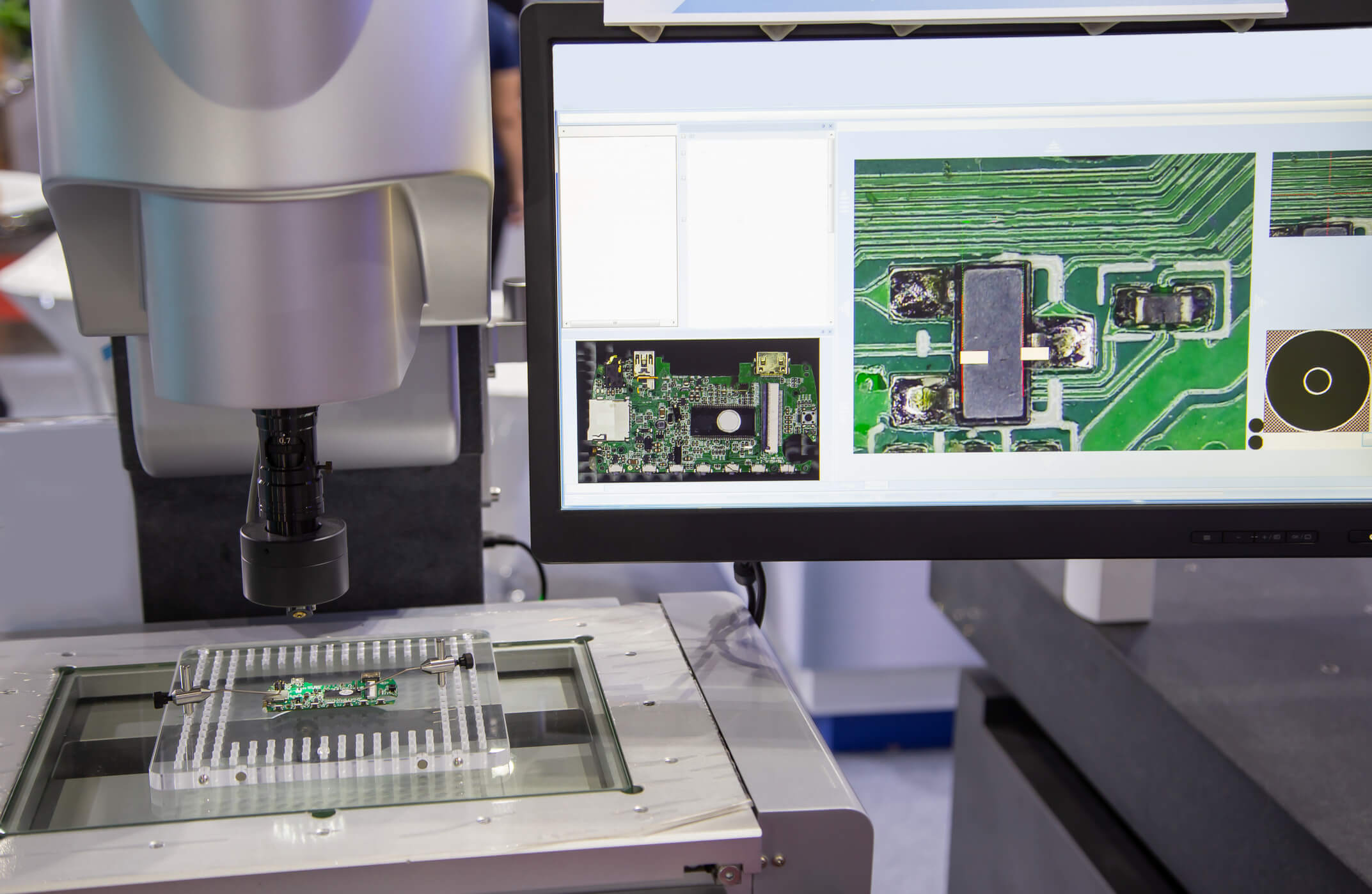
Automated Optical Inspection (AOI) is a key quality step in PCB manufacturing. It uses controlled lighting, calibrated cameras and software checks to confirm components are placed and soldered correctly. AOI provides consistent, repeatable inspection that supports reliable production, reduces rework and helps teams meet strict quality expectations.
In high-reliability environments, AOI gives engineering and quality managers confidence that every board has passed an objective review before it moves further into assembly or testing.
AOI is important because it delivers an objective way to verify placement accuracy and solder quality at speed, which reduces defect escapes and supports predictable production outcomes.
Quick Definition: Automated Optical Inspection Explained
Automated Optical Inspection is a machine-based visual check used to confirm that a PCB design has been assembled correctly. The system captures detailed images of the board, compares them to reference data and flags issues that could affect performance, reliability or safety.
AOI systems typically inspect each board in seconds, giving teams rapid feedback without slowing production.
In simple terms, AOI checks for:
- missing or misaligned components
- incorrect polarity or orientation
- solder issues such as bridges, opens or insufficient joints
- lifted leads and other placement faults
- component height variations or coplanarity issues
This provides a fast, consistent and objective way to verify quality, helping teams catch defects early and maintain stable production outcomes.
How Automated Optical Inspection Works
Automated Optical Inspection evaluates a PCB by capturing high-resolution images and analysing them against expected patterns. The system uses controlled lighting and calibrated cameras to highlight component edges, solder joints and surface features that indicate correct placement.
The software compares each captured image to reference data. This may include the original design files, a verified sample board or defined rules for component position and solder quality. Any variation outside the allowed tolerance is flagged for review.
These comparisons help reduce manual inspection workload and lower the risk of inconsistent visual checks.
AOI can operate in 2D or 3D.
- 2D AOI checks surface features such as presence, position and polarity.
- 3D AOI also includes height and volume measurements, which improve the accuracy of solder joint assessments and reduce false positives on complex assemblies.
This process enables early detection of placement and solder issues, supporting stable SMT production and reducing the chance of defects progressing to later stages.
Where AOI Fits in the PCB Assembly Process
Automated Optical Inspection is positioned at key stages of surface mounting technology production to verify quality before boards move forward. Its placement helps catch issues early, when they are faster and more cost-effective to correct.
Each stage also prevents defects from becoming embedded in later steps, reducing rework and improving throughput.
Common inspection points include:
- Solder Paste Inspection: Checks paste deposits for volume, alignment and coverage before components are placed.
- Pre-Reflow Inspection: Confirms that components are present, aligned and correctly oriented before soldering.
- Post-Reflow Inspection: Verifies solder joints, identifies lifted leads, bridges and insufficient solder after reflow.
- Final Assembly Checks: Provides an additional review for assemblies that require high reliability or compliance.
At Masters & Young, automated optical inspection forms part of a broader quality assurance workflow that also includes Flying Probe testing and functional checks. This combination helps ensure each board meets electrical, mechanical and reliability requirements before it is released to the next stage of production.
Defects AOI Can Detect
Automated Optical Inspection is designed to identify issues that affect placement accuracy, solder quality and overall board reliability. It highlights variations that fall outside defined tolerances, helping teams address problems before they progress further into PCB assembly or testing.
Common defects AOI detects include:
- missing components
- incorrect polarity or orientation
- misaligned or skewed parts
- tombstoning and lifted leads
- solder bridges and shorts
- insufficient or excess solder
- open solder joints
- wrong component values or package types
- surface contamination that affects performance
AOI also picks up subtle issues that are difficult to catch manually, such as small shifts in component height or weak solder joints on dense or complex boards. This makes it a dependable step for maintaining accuracy and supporting consistent production outcomes.
Advantages of Automated Optical Inspection
Automated Optical Inspection supports stable, high-reliability production by improving accuracy, reducing rework and strengthening documentation. These advantages directly influence product quality, project timelines and lifecycle cost.
Without AOI, minor placement or solder issues can progress into later stages, where they are more costly and difficult to repair.
Quality and Reliability Gains
AOI delivers consistent, objective inspection that is not influenced by fatigue or variation between operators. It identifies placement and solder issues early, reducing the chance of defects progressing into later stages where they are harder and more expensive to correct. This helps maintain predictable production quality across every batch.
Cost and Productivity Gains
By catching defects at the point of introduction, AOI reduces rework, scrap and slowdowns in downstream processes. Inspecting boards at speed supports efficient throughput and helps teams maintain stable lead times. These gains compound across large or repeated production runs, improving overall cost efficiency.
Compliance and Traceability Gains
Industries with strict quality requirements rely on documented evidence of consistent inspection. AOI supports this through repeatable checks, image logs and defined tolerances that align with standards such as IPC Class 3 and AS9100D. This level of traceability helps teams meet audit expectations and maintain process compliance.
Better Project Outcomes
AOI reduces the risk of field failures, early-life faults and warranty claims by ensuring each board is inspected against objective criteria. This improves confidence in every production run, supports more reliable product launches and provides engineering teams with stable, predictable output they can build on for future revisions.
2D vs 3D Automated Optical Inspection
AOI can operate in 2D or 3D, with each method offering different levels of detail and measurement capability. Understanding the distinction helps teams choose the right approach for their assembly requirements.
2D AOI captures top-down images to assess presence, position, polarity and basic solder quality. It is effective for boards with clear markings, standard component packages and lower density layouts. Most surface-level defects can be identified reliably through this method.
3D AOI measures height and volume, allowing the system to analyse solder joint shape, lead lift, coplanarity and variations in component height. This improves accuracy on dense or complex assemblies, reduces false positives and provides more insight into the condition of each joint.
For many applications, 2D AOI is sufficient. Projects that involve fine-pitch parts, BGAs or higher reliability requirements benefit from the additional data captured through 3D AOI.
How PCB Design Choices Influence AOI Accuracy
The effectiveness of Automated Optical Inspection depends partly on how the PCB is designed. Clear markings, consistent spacing and defined reference points help the system capture accurate images and assess each component correctly.
Key design factors that improve AOI performance include:
- Fiducials: Precise reference points that help the system align each image and maintain inspection accuracy across every board.
- Component Spacing: Adequate room around parts reduces shadowing and makes it easier for AOI to detect edges, polarity markers and solder joints.
- Silkscreen Clarity: Clear outlines, labels, and polarity indicators support faster and more accurate recognition.
- Polarity Markings: Well-defined orientation marks help AOI confirm each component is placed in the correct direction.
- Solder Mask Openings: Properly sized and positioned openings improve visibility of solder joints, supporting reliable defect detection.
Integrating these considerations during the design stage helps AOI operate with greater precision. At Masters & Young, these elements are reviewed during the Define and Design phases, ensuring each board is optimised for efficient inspection and consistent manufacturing outcomes.
Why AOI Matters in High-Reliability Industries
Automated Optical Inspection plays a significant role in sectors where product performance, safety and compliance cannot be compromised. These industries rely on consistent inspection and clear documentation to confirm every board meets defined standards before it reaches the field.
Defence and Aerospace
Electronics used in defence and aerospace must withstand demanding conditions and maintain long-term reliability. AOI supports this by providing an objective review of solder joints, component placement and assembly quality, reducing the chance of early-life faults or intermittent failures.
Medical Devices
Medical electronics require stable performance and traceable inspection records. AOI creates repeatable logs and image data that support compliance, help address audit requirements and ensure assemblies meet the expectations of regulated environments.
Mining and Industrial Systems
Equipment used in harsh operating environments depends on robust electronics. AOI helps identify subtle defects that could impact durability or cause unexpected downtime, supporting more predictable maintenance schedules.
Advanced Manufacturing and Automation
High-density boards with fine-pitch components benefit from the consistent accuracy AOI provides. This helps maintain performance across large production runs and supports long-term system stability.
Across all high-reliability applications, AOI reinforces quality at a stage where defects are most cost-effective to correct, strengthening overall project outcomes.
Start Your Project with a High-Reliability Manufacturing Partner
Automated Optical Inspection is one part of a broader quality framework that supports accurate, consistent and reliable PCB production. When combined with strong design practices, controlled assembly processes and additional testing methods, it helps reduce defects early and maintain stable outcomes across every batch.
Masters & Young integrates AOI with Flying Probe testing, functional checks and standards-driven workflows under AS9100D and IPC Class 3. This approach gives engineering and quality teams confidence that each board has been reviewed against clear criteria before it moves to the next stage.
If you are planning a new project or reviewing your current manufacturing approach, our Brisbane-based team can support the full process from design through to production and inspection.
Reach out to discuss your requirements and move forward with a partner focused on reliability.