

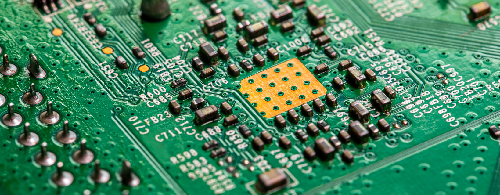
Modern electronics are being asked to do more in less space. Products need to be smaller, smarter, lighter and more capable, while internal components are often becoming denser and more difficult to route.
For many projects, a standard PCB layout is enough. Some products can also be handled well with a standard multilayer PCB. HDI PCB design becomes relevant when the product’s size, component density, routing requirements or performance goals push beyond what those standard structures can comfortably support.
A great HDI PCB design is not simply the smallest or most advanced board. It is the board architecture that helps the product achieve its required size, performance, reliability, manufacturability and commercial goals.
For product teams, that can mean fitting more functionality into a smaller enclosure, supporting fine-pitch components, reducing mechanical compromises, improving layout efficiency or creating a stronger pathway from prototype to production.
What Is an HDI PCB?
An HDI PCB is a high-density interconnect printed circuit board designed to fit more electrical connections into a smaller physical space.
HDI PCBs use finer lines, smaller spaces and advanced interconnect methods to support compact layouts. These can include microvias, blind vias, buried vias and via-in-pad design.
These features matter because they create connection paths between layers without using as much board space as traditional through-hole vias. That gives the designer more room for component placement, signal routing and compact board architecture.
In many projects, an HDI PCB is an advanced multilayer PCB that uses higher-density interconnect structures to support complex routing, compact components and stronger use of available board space.
When Does HDI PCB Design Make Sense?
HDI PCB design makes sense when the product needs more density, routing flexibility or compact functionality than a standard PCB can provide.
HDI may be worth considering when:
- The board size is fixed, but functionality needs to increase
- Fine-pitch components or BGAs are limiting routing space
- Traditional through-hole vias take up too much board area
- The product enclosure cannot be increased
- Shorter interconnects would support better layout efficiency
- Multiple functions need to fit into one compact board
- The product needs a smaller or lighter form factor
- The design needs a clearer path from compact prototype to production
This does not mean HDI is always the answer. For an industrial controller with a larger enclosure and moderate routing demands, a standard multilayer PCB may still be the better commercial choice. For a compact medical device, wearable product or sensor-based system with strict size limits, HDI may be justified because the physical product cannot work as intended without a denser board structure.
A useful way to think about HDI is this: the board should become more advanced only when the product goal requires it.
What Makes a Great HDI PCB Design?
A great HDI PCB design starts with the product goal. The board should support what the product needs to do, how it needs to fit, how it will be manufactured and how it will perform in real use.
The Right Level of Density
Good HDI design uses density where it creates clear value. The aim is not to add layers, microvias or via-in-pad structures because they sound advanced. The aim is to create a board that gives the product the space, routing and functionality it needs.
A useful test is whether each HDI feature helps reduce board size, improve routing, support a key component or create a more practical production pathway.
For some products, full HDI may be the right approach. For others, a simpler multilayer structure may provide the best balance of performance, cost and manufacturability.
Clear Component and Routing Strategy
HDI PCB design is often driven by component placement. Fine-pitch components, dense ICs, compact modules and connectors can make escape routing difficult on a standard board.
A strong design considers component placement, routing paths and internal connections together. This is especially important when key components need to sit close together, align with enclosure features or avoid heat, noise or mechanical constraints.
The layout should support the product, not fight against it. When component placement and routing are planned together, the board has a better chance of meeting both electrical and mechanical requirements.
Strong Board Architecture
Once HDI is justified, the internal board architecture becomes a major design decision. This includes layer count, material selection, power and ground planning, signal routing, via strategy and stack-up.
The best HDI design is planned as a complete structure, not as a standard layout with advanced features added late in the process.
This matters because board architecture affects more than the PCB. It can influence enclosure design, assembly approach, test access, production cost and the ability to manufacture the product consistently.
Manufacturability From the Start
A great HDI PCB design is not only compact. It is also buildable, inspectable, testable and repeatable.
Manufacturing input should shape decisions around materials, layer count, via structures, minimum trace and space, assembly needs and inspection access. This helps keep the design practical as it moves from prototype to production.
For example, a board may be technically possible to design, but difficult or expensive to manufacture repeatedly if the stack-up, microvia structure or material choices are not aligned with the manufacturing process.
Alignment With Commercial Goals
The right HDI design supports the business case behind the product. It balances size, performance, reliability, cost, production volume and time to market.
The smallest board is not always the best board. The best board is the one that helps the product perform properly while remaining commercially viable to manufacture.
For a compact medical device, higher density may be justified because the enclosure size and user experience depend on it. For a larger industrial product, the better decision may be a less complex board that still meets the functional requirements.
Planning the HDI Board Architecture: Stack-Up, Layers and Via Strategy
In HDI design, stack-up is part of the board architecture. It defines how internal layers, dielectric materials, signal routes, power planes, ground planes and via structures work together.
This is also where the term HDI multilayer PCB often appears. An HDI multilayer PCB is the finished board structure. The HDI PCB stack-up is the internal plan used to build that structure.
Stack-up is most relevant when the board uses multiple layers. In HDI projects, it becomes a central design decision because the internal layer plan affects density, routing, performance and manufacturing feasibility.
Stack-up decisions can influence:
- How much routing space is available
- How easily dense components can be connected
- How power and ground are distributed
- How signal paths are managed
- How heat moves through the board
- How practical the board is to manufacture
- How cost-effective the final structure is
Via strategy is also central to HDI design. Microvias, blind vias, buried vias and via-in-pad structures can help create shorter and more efficient connections between layers. This can improve routing around dense components and free up space that would otherwise be taken by traditional through-hole vias.
The goal is not simply to add more layers. The goal is to create a board structure that supports the product’s required function, available space, assembly process and production pathway.
For products that need a compact and capable board structure, HDI PCB design can provide more flexibility than standard layouts.
How HDI Design Supports Product Outcomes
HDI PCB design can support better product outcomes when density and space are part of the design challenge.
Smaller Physical Products
HDI can help reduce board size, which can support smaller enclosures, lighter devices and more refined product design. This is valuable when the external size of the product directly affects usability, portability or installation.
More Functionality in the Same Space
Product teams often want to add more capability without increasing the size of the device. HDI can help fit more components, connections and functions into a limited board area.
This can support products that combine processing, sensing, communication, power management and control functions in one compact design.
Better Layout Flexibility
HDI can give designers more freedom when working around enclosure limits, connector positions, mechanical features and component placement requirements.
This can reduce the need for awkward compromises between the electronic design and the physical product design.
Shorter and More Efficient Connections
Microvias and compact interconnects can help create shorter paths between layers and components. This can support cleaner routing and better use of available space.
For some designs, this can also help support signal integrity and layout efficiency, especially where dense components need to connect across multiple layers.
Stronger Prototype-to-Production Planning
A well-planned HDI design can help teams move from prototype to production with fewer structural changes. This is especially important when the board is central to the final product’s size, function and assembly process.
When planned well, HDI design can help bridge the gap between an ambitious product concept and a board that can be manufactured with confidence.
HDI PCB Design for Manufacturability
HDI PCB design for manufacturability (DFM) is about making sure the board can be built, assembled, inspected and repeated without unnecessary complexity.
This starts with choosing the simplest HDI structure that meets the product goal. More layers and more advanced via structures can increase capability, but they should have a clear purpose.
Key manufacturability considerations include:
- whether the chosen HDI stack-up is realistic for production
- whether the microvia structure can be produced consistently
- whether materials are suitable and available
- whether minimum trace and space requirements are practical
- whether drill sizes and via structures are achievable
- whether assembly requirements have been considered
- whether inspection access is available where needed
- whether test points can be included where practical
- whether the prototype design can support future production
This matters because a prototype-only mindset can create problems later. A board may prove a concept, but it still needs major changes before it is commercially practical to manufacture.
Good DFM keeps the product pathway in view from the start. It asks not only “can this be designed?” but also “can this be built, assembled, inspected and repeated in a way that supports the business goal?”
DFM does not limit design ambition. It helps make sure the design ambition can be delivered in a practical, controlled and commercially sensible way.
Masters & Young supports PCB design and manufacturing projects with engineering and manufacturing insight, helping teams consider the design and production pathway together.
Where HDI PCB Design Is Commonly Used
HDI PCB design is commonly used in products where compact size, high component density and reliable performance need to work together.
It is often used in smartphones, tablets, wearables, cameras, IoT devices, sensor systems, compact computing modules and telecommunications hardware. These products need more functionality in smaller physical spaces, which makes routing efficiency and board architecture important.
HDI is also relevant in automotive electronics, robotics, automation systems and industrial control products where electronic assemblies may need to fit inside defined mechanical spaces while supporting control, sensing, communication or processing functions.
In high-reliability applications, HDI can support compact and capable electronics for medical electronic design and manufacturing, as well as defence and aerospace electronic manufacturing. In these environments, the value of HDI comes from matching board density with reliability, manufacturability and application requirements.
Across all of these use cases, HDI is most useful when standard PCB structures cannot provide the density, size or routing flexibility the product needs.
What To Discuss With an HDI PCB Design Partner
Before finalising an HDI PCB design, it helps to discuss the product goals and design constraints early.
These questions help clarify whether HDI is the right approach, what level of board complexity is justified and whether the design can move from prototype to production without needing a major rethink.
Useful questions include:
- What is driving the need for HDI?
- Which components are creating the routing or density challenge?
- What board size or enclosure limits apply?
- What performance requirements need to be supported?
- What production volumes are expected?
- What reliability requirements apply?
- What stack-up and via structures make sense?
- How will the board be assembled, inspected and tested?
- Can the design approach support prototype and production?
These questions help turn HDI from a technical concept into a practical product decision. They also help product teams compare suppliers on more than price. The right partner should be able to discuss design, manufacturing, inspection and production requirements together.
How Masters & Young Can Support HDI PCB Projects
Masters & Young supports Australian electronics projects from early design decisions through to prototyping, assembly, testing and production. For HDI PCB projects, this means our team can help with more than layout alone.
We can assist with product requirements, board architecture, HDI stack-up planning, via strategy, design for manufacturability, component selection, assembly requirements and production planning. This helps product teams consider the complete pathway from concept or prototype through to a finished, tested electronic product.
Our Brisbane-based facility supports HDI PCB design and manufacturing, SMT and through-hole assembly, prototype builds, production runs, testing and quality control. For complex boards, this can include practical support around inspection, functional testing, X-ray inspection, BOM review, component sourcing and production documentation.
This end-to-end capability is especially valuable when the HDI PCB forms part of a broader product, not just a standalone board. Our team can help align the PCB design with the enclosure, firmware, assembly process, testing requirements and commercial production goals.
We work across advanced electronics applications, including defence, aerospace, medical, industrial, mining, automotive, communications and commercial technology projects.
Need Support With an HDI PCB Project?
If your product needs more functionality in less space, early engineering and manufacturing input can help you choose the right board structure before prototype or production.
Masters & Young can help assess your product goals, HDI stack-up, via strategy, assembly needs, testing requirements and production pathway so your design is practical, buildable and aligned with your commercial goals.
Speak with the Brisbane-based team about your next electronics project.