

The mining sector has increasingly embraced high-power LED lighting solutions to enhance safety, productivity, and energy efficiency in challenging underground environments. At the core of these sophisticated lighting systems lies a critical component: Aluminium-Backed Printed Circuit Boards (PCBs). These specialised PCBs are instrumental in ensuring optimal performance and reliability of LED lighting in mining applications.
A primary challenge in high-power LED applications is effective heat dissipation. Aluminium-Backed PCBs demonstrate exceptional capabilities in this domain, delivering superior thermal management compared to conventional FR4 PCB design.
Heat Dissipation Advantages:
Through effective thermal management, Aluminium-Backed PCBs substantially extend LED component lifespans, minimising maintenance requirements and operational disruptions in mining activities.
Enhanced Durability for Harsh Mining Environments
Mining environments present notorious challenges, including exposure to particulates, moisture, and constant vibration. Aluminium-Backed PCBs feature robust construction engineered to withstand these demanding conditions.
Durability Benefits:
This enhanced durability results in reduced system failures and replacement requirements, ensuring dependable illumination in critical mining zones.
Improved Safety Through Better Lighting
Safety remains paramount in mining operations, with proper lighting playing a vital role. Aluminium-Backed PCBs enable the implementation of high-power LED lighting systems that deliver superior illumination.
Safety Enhancements:
By facilitating more powerful and efficient LED lighting, Aluminium-Backed PCBs directly contribute to enhanced workplace safety for mining personnel.
Energy Efficiency and Cost Savings
The mining industry consistently seeks methods to reduce energy consumption and operational expenses. Aluminium-Backed PCBs support this objective by enabling more efficient LED lighting solutions.
Efficiency Advantages:
These efficiency advantages translate into substantial cost reductions over time, making Aluminium-Backed PCB design a prudent investment for mining operations.
Customisation and Flexibility
Each mining operation presents distinct lighting requirements. Aluminium-Backed PCBs provide the versatility needed to develop bespoke lighting solutions.
Customisation Options:
This adaptability enables mining companies to develop lighting solutions perfectly aligned with their operational requirements. In conclusion, Aluminium-Backed PCBs represent a crucial element in developing high-power LED lighting for the mining sector. Their exceptional thermal management, resilience, and adaptability make them the optimal choice for creating safer, more efficient, and cost-effective lighting solutions in challenging mining environments. As the industry continues to prioritise safety and efficiency, the significance of Aluminium-Backed PCBs in mining applications will undoubtedly continue to grow.
In today’s high-speed electronic systems, electromagnetic compatibility challenges can make or break a product’s success. Studies show that over 50% of electronic products fail their initial EMC testing, leading to costly redesigns and delayed market launches.
However, achieving electromagnetic compatibility doesn’t have to be a matter of trial and error. Specifically designed PCB layout techniques and methodical design approaches can effectively minimise EMI issues from the start. This comprehensive guide examines proven strategies for EMI design and demonstrates how proper PCB layout practises ensure first-pass EMC compliance.
Understanding EMC Design Fundamentals
Electromagnetic compatibility represents the cornerstone of reliable electronic design, essentially determining how well devices operate in their intended environment without causing or experiencing interference. Understanding EMC fundamentals begins with recognising that every electronic device must both limit its electromagnetic emissions and maintain immunity to external interference sources.
Key principles of electromagnetic compatibility
The foundation of EMC design rests on three fundamental principles:
Critical factors affecting EMC performance
Notably, several critical factors influence EMC performance in PCB design. The selection of components and their placement significantly impacts electromagnetic emissions, with surface mount components offering superior EMC performance compared to radial and axial leaded alternatives. Furthermore, proper decoupling capacitor implementation proves crucial, as these components should be placed as close as possible to each IC to effectively reduce switching noise propagation across the board.
Impact of PCB layout on electromagnetic emissions
PCB layout fundamentally shapes electromagnetic emissions and system immunity. Studies indicate that boards designed without EMC considerations often fail initial compliance testing. Consequently, implementing proper layout techniques from the start becomes essential. The arrangement of ground planes, signal routing, and component placement directly influences the electromagnetic field containment.
A well-designed PCB layout incorporates strategic ground plane placement and maintains controlled impedance for high-speed signals. In essence, the layout must ensure that return currents follow their intended paths, as improper return paths can create unintended antennas that increase electromagnetic emissions.
Implementing Essential PCB Layout Techniques
Proper PCB layout serves as the foundation for achieving optimal electromagnetic compatibility in electronic designs. The implementation of essential layout techniques requires careful attention to component placement, ground plane design, and power distribution strategies.
Optimal component placement strategies
Board segregation plays a vital role in minimising electromagnetic interference. The layout should be divided into distinct sections based on circuit functionality:
Ground plane design and implementation
A well-designed ground plane forms the cornerstone of EMC-compliant PCB design. Studies indicate that maximising the ground area on a PCB notably reduces ground inductance, thereby minimising electromagnetic emissions and crosstalk. Moreover, implementing a solid, unbroken ground layer provides the least impedance value for signal returns.
Power distribution network optimisation
The Power Distribution Network (PDN) demands meticulous attention to ensure stable power delivery across the board. Particularly, the strategic placement of decoupling capacitors proves crucial – they should be positioned as close as possible to IC power pins to minimise current loops. Additionally, utilising multiple decoupling capacitors with varying capacitance values addresses a broader frequency range of noise.
For optimal PDN performance, trace routing requires careful consideration. Power and ground traces should run parallel when a separate power plane isn’t feasible. The implementation of wide trace widths with low-resistivity materials enables enhanced current flow, while multiple power planes result in reduced impedance paths.
Mastering Signal Routing for EMC
Signal routing represents a critical aspect of electromagnetic compatibility design, demanding careful attention to both trace layout and signal integrity. Indeed, proper routing techniques can significantly reduce electromagnetic interference while ensuring reliable signal transmission.
High-speed signal routing guidelines
Successful high-speed signal routing begins with minimising trace lengths and controlling impedance. According to industry standards, high-speed traces should maintain a separation of at least 2 times the trace width to reduce crosstalk. For optimal performance, consider these essential guidelines:
Differential pair routing techniques
Differential pair routing offers superior noise immunity and enhanced signal integrity. Important to realise, differential pairs should be routed as close together as possible to achieve optimal coupling. The traces in differential pairs must maintain equal lengths to ensure proper signal timing, with high-speed USB requiring length mismatches no greater than 150 mils.
Return path considerations
In light of EMC requirements, return path design proves crucial for minimising electromagnetic emissions. The return current always follows the path of least impedance, accordingly, providing a clear return path directly underneath signal traces becomes essential. At higher frequencies, the reactive component becomes more significant than resistance, making the loop inductance a critical factor.
The design must ensure continuous return paths, especially when signals transition between layers. For optimal performance, ground vias should be placed close to signal vias, reducing impedance discontinuities and minimising reflections. Furthermore, any slots or gaps in the ground plane should be avoided as they can create unintended antennas and increase emissions.
Applying Advanced EMC Design Strategies
Advanced electromagnetic compatibility strategies elevate PCB design beyond basic layout techniques, focusing on sophisticated methods to achieve optimal EMI performance. Proper implementation of these strategies often determines whether a board passes EMC testing on the first attempt.
Shielding and filtering techniques
Physical shielding serves as a crucial defence against electromagnetic interference. For optimal results, consider these proven shielding methods:
Stackup optimisation methods
Stackup configuration fundamentally influences EMC performance through proper layer arrangement and impedance control. A well-designed stackup minimises electromagnetic interference by optimising signal and return planes. Subsequently, maintaining controlled impedance becomes vital, notably for high-frequency signals where proper impedance control ensures signal integrity and minimal distortion.
Furthermore, sequential layer alignment proves essential, with high-speed signal layers strategically positioned below power planes to promote tight coupling and reduce electromagnetic interference. This arrangement effectively creates a shield against radiation from high-speed signals.
Decoupling and bypass techniques
Decoupling and bypass capacitors play distinct yet complementary roles in maintaining power integrity. Bypass capacitors should be positioned between an IC’s power supply pin and ground, therefore addressing voltage fluctuations specifically between the output pin and PCB ground plane.
Notably, for optimal performance:
The implementation of these advanced strategies requires careful attention to detail and thorough understanding of electromagnetic principles. Through proper execution, these techniques effectively minimise EMI issues while ensuring robust circuit performance.
Conclusion
Electromagnetic compatibility challenges need not derail electronic product development. Though studies show many products fail initial EMC testing, proper implementation of proven PCB design techniques significantly increases first-pass success rates.
Strategic component placement, thoughtful ground plane design, and careful signal routing form the foundation of EMC-compliant boards. These fundamentals, combined with advanced strategies like optimal stackup configuration and proper shielding, create robust designs that minimise electromagnetic interference.
Success lies in addressing EMC requirements early during the PCB design phase. Rather than treating electromagnetic compatibility as an afterthought, designers who embrace these proven techniques from the start save considerable time and resources. Most importantly, they deliver reliable products that perform as intended in real-world environments.
At Masters & Young, we recognize that Printed Circuit Board (PCB) assembly is a crucial phase in electronics manufacturing. As a leading electronic design and manufacturing company, we aim to help our clients make informed decisions by explaining the primary factors that influence PCB assembly costs.
Component Selection
The choice of components plays a significant role in determining the overall cost of PCB assembly. While the PCB substrate itself (whether FR-4, polyimide, or metal-core) contributes to the expense, it’s typically minor compared to the cost of components such as integrated circuits (ICs), resistors, capacitors, and connectors.
Design Complexity
The intricacy of your PCB design directly impacts the assembly cost. Multi-layer boards with high component density are naturally more expensive to produce than simpler, single-layer designs. At Masters & Young, we have the expertise to handle a wide range of design complexities, ensuring efficient assembly while maintaining competitive pricing.
Assembly Techniques
The choice between surface-mount technology (SMT) and through-hole assembly significantly affects the overall cost. SMT is generally more cost-effective for large-scale production, while through-hole assembly may be pricier due to its labor-intensive nature. Our team at Masters & Young is proficient in both techniques, allowing us to recommend the most suitable and cost-effective option for your project.
Quality Assurance
Rigorous testing and quality control are essential for high-quality PCB assembly. The extent of testing required, such as functional testing, in-circuit testing, and automated optical inspection, can impact the final cost. At Masters & Young, we prioritise thorough testing and compliance procedures to ensure you receive a reliable product, minimising the risk of costly defects in the long run.
Production Volume
The quantity of PCBs needed can significantly influence the per-unit cost. Larger production runs often benefit from economies of scale, potentially reducing the cost per board. At Masters & Young, we cater to both small batch productions and large-scale manufacturing, providing cost-effective solutions tailored to your specific needs.
Turnaround Time
The urgency of your project can affect the overall cost. Expedited services may incur additional charges due to the need for dedicated resources and potential overtime. We at Masters & Young strive to balance quick turnaround times with cost-effectiveness to meet your project deadlines without compromising quality.
By understanding these factors, you can make more informed decisions about your PCB assembly projects. At Masters & Young, we’re committed to providing high-quality, cost-effective PCB assembly services. Our advanced tools and expertise allow us to handle intricate designs while maintaining efficiency and quality.
For your next PCB assembly project, trust the experts at Masters & Young. Contact us today to discuss how we can streamline your electronic design and manufacturing needs.
As the landscape of global defense evolves, electronic warfare (EW) has emerged as a critical component of military strategy. In Australia, the need for advanced EW capabilities is increasingly recognized, particularly within the Australian Defence Force (ADF).
Masters & Young, a leading electronics engineering firm based in Logan City, Queensland, is at the forefront of this evolution, providing innovative solutions that bolster the ADF’s electronic warfare capabilities.
The Significance of Electronic Warfare
Electronic warfare encompasses a range of operations designed to exploit the electromagnetic spectrum (EMS) for military advantage. This includes disrupting enemy communications, gathering intelligence, and ensuring the effectiveness of friendly operations. Given the complexity and contested nature of the EMS, there is a pressing demand for technologies that can provide both offensive and defensive capabilities.
Masters & Young’s Role in Electronic Warfare
At Masters & Young, we specialize in designing and manufacturing sophisticated electronic systems that meet the unique requirements of the defense sector. Our contributions to Australia’s electronic warfare capabilities include:
Custom Electronics Development: We develop tailored solutions that address specific EW challenges faced by the ADF. Our engineering team collaborates closely with defense stakeholders to ensure our products align with operational needs.
High-Quality Prototyping: Our state-of-the-art facility allows us to produce prototypes rapidly, enabling quick iteration and testing of new technologies. This agility is vital in a field where rapid advancements are essential for maintaining operational superiority.
Advanced Research and Development: We invest in R&D to explore emerging technologies that enhance EW capabilities. By focusing on innovations such as sensors and electromagnetic spectrum management tools, we aim to provide solutions that offer strategic advantages.
Aligning with National Defense Initiatives
The recent launch of the AUKUS trilateral innovation challenge underscores the Australian government’s commitment to enhancing its electronic warfare capabilities through collaboration with allied nations. Masters & Young is poised to contribute significantly to these initiatives by leveraging our expertise in electronics manufacturing and design.Our involvement in such collaborative efforts not only strengthens our position within the defense industry but also ensures that we are aligned with national priorities. As part of our commitment to excellence, we adhere to rigorous quality standards such as IPC-A-610 and J-STD-001, ensuring that all our products meet military specifications.
As electronic warfare becomes increasingly vital to national security, Masters & Young stands ready to support the Australian Defence Force with innovative electronic solutions. Our dedication to quality, rapid prototyping, and tailored development positions us as a key player in enhancing Australia’s defense capabilities.
Contact M&Y for more information on how we can assist with your electronic warfare projects or any other defense-related initiatives. Together, let’s fortify Australia’s defense landscape through cutting-edge electronics engineering.
Furthermore, best practice dictates consolidating all input and output cables along a single board edge, rather than distributing them across multiple edges. This approach prevents potential differences between cables and minimises antenna-like structures that could propagate digital signals or noise.
Board segregation, alternatively referred to as board partitioning, represents a strategic methodology for organising various circuit components within a Printed Circuit Board (PCB) to maintain their isolation. This approach significantly enhances the board’s performance, particularly concerning EMI reduction. This methodology not only mitigates electromagnetic interference but also optimises the signal integrity of the PCB design.
The core principles underlying these methodologies encompass:
High-Speed vs. Low-Speed Signals and Their Harmonics
The primary concept addresses the management of high-energy harmonic content generated by rapidly switching signals and their rate of current variation over time. Higher rates of current variation produce increased harmonic energy within signals, thereby elevating radiation probability.
The secondary concept relates to how signal frequency influences return current behaviour. This occurs because signal propagation impedance comprises not only conductor resistance but also capacitance and, crucially, loop inductance. The inductive impedance component increases proportionally with signal frequency.
Differences in Return Paths
Understanding that current invariably follows the path of least impedance is crucial. At higher signal frequencies, return current closely tracks signal current to minimise inductive loops. Conversely, at lower signal frequencies, where inductance becomes negligible, the resistive impedance component dominates.
Design, validate, and verify the most sophisticated schematics. Learn More.
At this juncture, return current disperses across the conductor’s surface, seeking minimal resistance pathways. The critical consideration for PCB designers lies in understanding how signal frequency determines the return current’s path to its source.
As PCB design specialists, our primary objective is to minimise interference between these return currents, thereby preventing common-impedance coupling that could trigger electromagnetic emissions. We achieve this by establishing dedicated zones or sections within the PCB, each allocated to specific circuit types. This approach additionally reduces current loops, consequently diminishing radiation from differential-mode currents.
Whilst it may appear advantageous to implement a split in the Return Reference Plane (RRP) to enhance isolation between different circuit return current paths, this approach contradicts established EMC best practices. Such splits generate potential differences between metallic regions, effectively creating antenna-like structures that can amplify electromagnetic emissions in PCB design.
The industry’s premier PCB design ecosystem. Explore Solutions.
The optimal approach involves implementing a continuous, low-impedance return reference plane that facilitates natural return current pathways to their sources. This plane must maintain integrity without cuts, splits, or substantial gaps that could generate common-mode noise. Component placement should be strategically organised into distinct zones based on circuit functionality and type.
For mixed-signal PCBs, the recommended segregation typically comprises distinct zones: digital, power, analogue, input/output, and when required, filtering sections. The digital section warrants particular attention and should maintain significant distance from other components. Despite return current following signal traces closely, the substantial harmonic energy content inherent in these signals presents increased radiation potential and coupling risks with other board sections.
A common manifestation occurs when clock signals couple with other networks across the board, particularly in power and analogue sections where connected cables may function as unintended antenna structures, promoting emissions.
The input/output section proves crucial for multiple reasons: limiting noise injection into cables, enabling isolation through filtering techniques, and implementing shielding to mitigate external interference and board emissions. The layout must account for cables and peripheral structures. Digital sections should maintain maximum separation from input/output areas, ideally positioned within the board’s interior, away from edges, preventing high-energy harmonic coupling to cables or edge radiation.

Furthermore, best practice dictates consolidating all input and output cables along a single board edge, rather than distributing them across multiple edges. This approach prevents potential differences between cables and minimises antenna-like structures that could propagate digital signals or noise.
Adherence to these guidelines significantly enhances your PCB’s electromagnetic performance, reducing radiated emissions whilst strengthening resistance to external interference.
Our subsequent article will delve into optimal PCB stackup selection strategies for enhanced EMI performance and reduced risk profiles. Stay connected through our platforms and social media channels for continued insights into advanced PCB design methodologies.
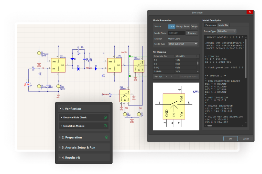
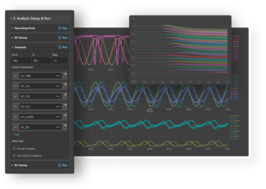
Delivering superior PCB design outcomes demands sophisticated tools that enable precise control across all design parameters. Our comprehensive PCB design ecosystem incorporates advanced layout capabilities, simulation features, and robust design validation tools, streamlining the board partitioning process whilst ensuring compliance with stringent requirements.
The sophisticated design rules engine and real-time simulation capabilities continuously verify adherence to specifications during PCB routing, maintaining exemplary design standards. Our secure cloud-based collaboration platform facilitates seamless file transfer to manufacturers, enhancing project coordination and fostering efficient teamwork throughout the development lifecycle.