

Plated through holes are a fundamental part of modern electronics. They are rarely visible in a finished product, yet they carry much of the signal and power that hold a printed circuit board together. For any business bringing a hardware product to market, understanding what plated through holes do, when they matter, and how they affect cost and reliability can make the difference between a board that lasts for years and one that fails in the field.
What Is a Plated Through Hole?
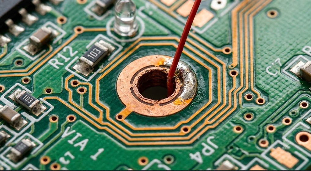
A plated through hole (PTH) is a hole drilled through a printed circuit board and then coated on its inner wall with a thin layer of conductive copper. That copper barrel turns a simple hole into an electrical connection, joining the copper layers and pads on different sides of the board so that current and signals can pass between them.
It helps to picture a circuit board as a stack of thin layers. On a single-sided board, all the copper sits on one face. The moment you need to connect the top of the board to the bottom, or to an internal layer buried inside a multilayer PCB, you need a reliable vertical path. Plating the inside of a drilled hole with copper creates exactly that path. Without it, the hole is just an empty gap.
Plated through holes serve two broad purposes:
- The first is to mount and connect components whose leads pass right through the board, which is the basis of through-hole assembly.
- The second is to act as vias, the small plated holes that connect one copper layer to another without holding a component at all.
Both rely on the same underlying idea: a clean, drilled hole with a continuous, well-bonded copper wall.
How Plated Through Holes Are Made
The process sits at the heart of PCB design and manufacturing and follows a well-defined sequence. Understanding the steps helps explain why quality control matters so much.
First, the holes are drilled through the board, either mechanically or with a laser, for the finest features. A freshly drilled hole has bare, non-conductive walls made of the board’s base material, so on its own, it cannot carry current.
Next comes desmear and deburring, which clean the hole walls and remove the residue left by drilling. The walls are then treated so that copper will adhere to them. A very thin conductive seed layer is applied through a process called electroless copper deposition, giving the walls just enough conductivity to accept electroplating.
The board then goes through electroplating, where a thicker, robust layer of copper is built up on the hole walls until the barrel reaches the required thickness. Finally, a surface finish is applied to protect the exposed copper and to help components solder cleanly later on.
Each of these steps has to be controlled tightly. A hole that is drilled off-centre, plated too thin, or contaminated during preparation can create a weak joint that passes initial inspection but fails under thermal or mechanical stress. This is why manufacturers with strong in-house quality assurance processes, including automated optical inspection and X-ray inspection, catch problems that would otherwise reach the customer.
Plated Through Holes Versus Surface Mount Technology
Many business decisions about a board come down to the balance between through-hole technology and surface mount technology (SMT). The two approaches are not rivals so much as complementary tools, and most modern products use a mix of both.
Surface-mount components sit directly on the surface of the board and are soldered to pads without passing through it. SMT enables smaller, denser designs, faster automated placement, and higher component counts, which is why it dominates high-volume consumer electronics. Plated through holes, by contrast, physically anchor a component’s leads through the board, creating a mechanically strong joint that resists vibration, shock, and repeated handling.
That mechanical strength is the key reason plated through holes remain essential. Connectors that get plugged and unplugged, large capacitors, transformers, power terminals, and any component that takes physical strain all benefit from the firmer hold of a through-hole joint. A design that leans entirely on surface mounting can struggle in demanding environments, while one that uses plated through holes where they count tends to be far more durable.
In practice, the right choice depends on the product. A skilled manufacturer will recommend through-hole, surface mount, or a mixed-technology build during design review, weighing reliability, size, cost, and production volume. Getting this decision right early, ideally while the schematic design is still taking shape, avoids expensive rework later.
Why Plated Through Holes Matter for Reliability
For businesses in high-reliability sectors, the quality of plated through holes is not a technical footnote. It is central to whether a product survives its intended life.
Boards used in defence and aerospace applications face extreme temperatures, vibration, and long service lives, where a single failed connection can have serious consequences. Equipment built for mining has to withstand dust, shock, and heavy operational loads. Devices in the medical field must perform consistently and predictably every time they are used. In each case, the integrity of the plated barrel and its bond to the surrounding copper is what keeps the circuit intact.
Plated through holes are also subject to thermal cycling. Every time a board heats up and cools down, the copper barrel and the board material expand and contract at slightly different rates. Over thousands of cycles, a poorly plated hole can crack. This is why plating thickness, copper quality, and adherence to standards such as IPC Class 2 and Class 3 are so closely monitored. Higher classes demand thicker, more robust plating precisely because the applications cannot tolerate failure.
The Role of Plated Through-Holes in Multilayer and Complex Boards
As products become more sophisticated, boards gain more copper layers, and plated through holes take on an even bigger role. In a multilayer PCB, plated holes connect not just the outer surfaces but the internal layers hidden within the stack, routing signals and power exactly where they are needed.
More advanced designs introduce different types of plated connections. Through-hole vias run the full thickness of the board, while blind and buried vias connect only some of the layers. In high-density interconnect (HDI) PCBs, microvias created by laser drilling allow extremely fine, compact routing that would be impossible with mechanical drilling alone. For high-speed PCB designs, the placement and construction of plated through holes even affect signal integrity, because each hole introduces small electrical effects that must be managed carefully.
The more layers and the higher the performance you demand, the more your product depends on precise, well-controlled plating, and the more it matters to work with a manufacturer that has genuine multilayer and HDI capability in-house.
Summarising Plated Through Holes
Plated through holes are a small feature with an outsized influence on how well an electronic product performs and endures. They connect layers, anchor components, and carry the mechanical and electrical loads that keep a board working in the real world. For businesses, the practical lesson is that plating quality is worth paying attention to, especially in demanding applications and in complex multilayer designs where there is little room for error.
Masters & Young has been designing and manufacturing electronics in Brisbane since 1997, with in-house SMT and PTH production lines, AS9100D and ISO 9001:2015 certification, and experience across defence, aerospace, medical, mining, and industrial applications. If you are planning a new product or refining an existing one, get in touch with our team to talk through the right approach for your board.