

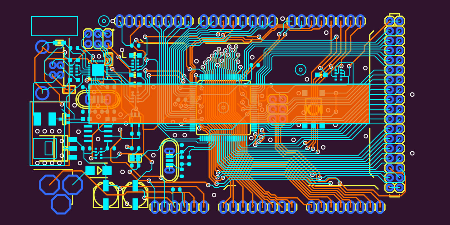
High-speed PCB design is about more than connecting fast components on a circuit board. It is about controlling how signals, power, materials and physical layout work together so the board performs reliably in the final product.
This matters most before a PCB moves into prototype or manufacturing. Early decisions around impedance, stack-up, routing, grounding, materials and testing can influence signal quality, electromagnetic interference (EMI) performance, production repeatability and the confidence a project team has in its prototype results.
For product teams, this can mean fewer late design changes, clearer validation results and a smoother pathway from engineering review to production.
When Does a PCB Become High-Speed?
A PCB becomes “high-speed” when the physical layout of the board starts to affect signal behaviour. This can happen when signals have fast rise times, long trace lengths, dense routing, strict timing requirements or sensitivity to impedance, crosstalk and electromagnetic interference.
This is not only about clock frequency. A board with fast digital interfaces, communications modules, high-speed memory, RF sections or dense processor layouts may need high-speed PCB design considerations even if the end product is not described as a “high-speed” device.
At this point, copper traces no longer behave like simple connections. They act more like transmission paths, where trace geometry, layer structure and return paths influence the signal.
That is why high-speed PCB design needs a planned approach from the start. The design needs to account for signal integrity, power stability, manufacturability and testing before the board is built.
What Great High-Speed PCB Design Needs To Control
A Great high-speed PCB design controls the board conditions that affect signal behaviour and production reliability.
These include:
- Controlled impedance
- Clear return paths
- Reduced crosstalk
- Stable power distribution
- Practical via design
- Suitable PCB materials
- Routing that supports timing requirements
- Layouts that can be manufactured consistently
These factors are connected. Stack-up affects return paths. Return paths affect signal integrity. Material selection can influence performance, cost and manufacturability. Power stability can affect whether signals behave consistently across operating conditions.
This is why high-speed PCB design needs to be reviewed as a complete system, rather than a group of isolated layout tasks.
Key Design Factors That Shape Performance
High-speed PCB performance depends on how the schematic, layout, stack-up, components, materials and manufacturing requirements work together. The following areas usually need careful attention before the prototype or production.
Controlled Impedance
Controlled impedance helps maintain consistent signal behaviour along a trace. When impedance is properly specified and manufactured, signals are more likely to move through the board with less reflection, distortion or loss.
This requires careful control of trace width, trace spacing, dielectric material, copper thickness and layer arrangement. It also requires coordination with the manufacturer so the finished board matches the design intent.
If controlled impedance is required, it should be specified and checked early. It should not be treated as an assumption in the layout file.
For example, a communications device with fast digital interfaces may need controlled impedance to support stable signal transfer between components.
Stack-Up Design
The PCB stack-up defines how copper layers, dielectric materials, signal layers, power planes and ground planes are arranged inside the board.
For high-speed designs, stack-up affects signal integrity, return paths, EMI control, power delivery, routing density and manufacturability. In many cases, a two-layer board does not provide enough control for fast signals or dense layouts.
The goal is not always to increase layer count. The goal is to choose a layer structure that gives signals, power and ground the support they need without adding unnecessary cost or production complexity.
For compact or performance-sensitive products, multilayer PCB design can support cleaner routing, stronger reference planes and better use of available board space.
Trace Routing and Length Matching
High-speed signals are sensitive to physical routing. Trace length, spacing, bends, stubs and layer transitions can all affect timing and signal quality.
Length matching matters when related signals need to arrive at a component at the same time. If signals arrive at different times, the design may experience timing skew. This can affect memory interfaces, processors, communication buses and synchronised data paths.
For project teams, this matters because timing issues can make prototype results inconsistent and difficult to interpret. Good routing supports more predictable board behaviour during validation.
Grounding and Return Paths
Every signal needs a return path. In high-speed PCB design, that return path is part of the signal loop.
A clear return path helps reduce noise, unwanted radiation and signal distortion. Ground planes, reference layers, via placement and routing decisions all influence how signals return through the board.
Return paths should be considered during stack-up and routing decisions, not checked only after the layout is nearly complete. This is especially important in dense boards where signals may change layers or pass near split planes, connectors or high-current areas.
Power Integrity
High-speed circuits need stable power to operate reliably. Power integrity depends on plane design, decoupling capacitor placement, component selection and current flow.
Even when signal routing is well planned, unstable power can cause noise, timing variation or inconsistent behaviour across operating conditions. This can affect processors, communications modules, high-speed ICs and fast-switching components.
A strong power strategy helps the board behave more consistently during testing and real use.
Material Selection
PCB material affects dielectric performance, signal loss, thermal behaviour, mechanical stability and manufacturability.
A material that suits a standard PCB may not suit a high-speed or high-frequency design. The right choice depends on signal speed, operating environment, thermal requirements, mechanical constraints, budget and expected production volume.
Material selection should consider performance and supply availability. An ideal material on paper still needs to suit the project’s lead time, cost target and manufacturing pathway.
Why Design Review Matters Before High-Speed PCB Prototyping
A design review before fabrication gives the project team a chance to check signal, stack-up, routing, material and manufacturability decisions while they are still easier to adjust.
A useful review may include:
- Layout review
- Impedance checks
- Stack-up review
- Component placement review
- Power and ground review
- Manufacturability feedback
- Assembly and testing considerations
This is valuable because prototype testing should help validate the product, not uncover avoidable design issues that could have been addressed earlier.
For example, a review may confirm whether the stack-up supports the intended return paths, whether trace geometry suits the required impedance, or whether routing around dense components could create avoidable crosstalk.
From a commercial perspective, design review can support clearer prototype results, fewer board revisions and a more confident move toward production.
How High-Speed PCB Design Supports Product Outcomes
High-speed PCB design directly affects how well the electronics support the final product.
More Predictable Prototype Results
A well-planned board gives teams more reliable data during prototype testing. This makes it easier to confirm whether the product concept, firmware, components and PCB layout are performing as intended.
Stronger Signal Integrity
Signal integrity supports stable communication between components. This is important in products that rely on processors, high-speed memory, communications modules, sensors, RF sections or synchronised data movement.
Better EMI Control
High-speed signals can increase EMI pressure if routing, grounding and stack-up are not planned well. Good board design can help reduce unwanted emissions and support a cleaner path through validation.
Smoother Production Planning
A board designed with manufacturing, assembly and testing in mind is easier to move beyond prototype. This is especially valuable for products that need repeatable manufacturing, customer trials, regulatory testing or staged production after validation.
Better Fit for Compact or Dense Products
In compact products, the PCB often needs to work around enclosure shape, connector placement, heat sources, mounting points and user-facing design requirements. High-speed PCB design can help align electrical performance with the physical product constraints.
Where High-Speed PCB Design Is Commonly Used
High-speed PCB design is relevant wherever signal performance, data transfer, timing or EMI control affects the product.
It is commonly used in communications equipment, embedded computing systems, robotics, sensor platforms, test equipment, industrial control systems, IoT devices, imaging systems, automotive electronics and advanced commercial products.
It is also important in high-reliability sectors. In defence and aerospace electronic manufacturing, boards may need to support dependable operation, repeatable manufacturing and clear documentation. Signal stability, EMI control and production consistency can form part of the broader product requirement.
In medical electronic design and manufacturing, PCB reliability can support device accuracy, safety and long-term performance. Design choices need to support dependable operation under real-use conditions.
The common thread is not the industry alone. It is the need for a board that can support fast or sensitive signals while remaining practical to build, test and manufacture.
What To Discuss With a High-Speed PCB Design and Manufacturing Partner
A high-speed PCB project benefits from a partner who can consider design, manufacture, assembly and testing together. The right questions can help product teams compare capability beyond price.
Design Capability
- Have they worked with similar signal speeds or application requirements?
- Can they advise on impedance, stack-up, materials and routing?
- Can they review signal integrity, return paths and power integrity before fabrication?
Manufacturing Capability
- Do they understand design for manufacturability?
- Can they support prototyping, assembly, testing and production?
- Can they help confirm whether the chosen materials and stack-up suit the production pathway?
Project Fit
- Do they have experience with high-reliability or performance-sensitive applications?
- Will engineering and manufacturing teams work together?
- Can they help the design move from prototype to production without unnecessary rework?
These questions help product teams avoid treating high-speed PCB design as a layout-only task. A high-speed board needs to be designed, built, tested and repeated with confidence.
How Masters & Young Supports High-Speed PCB Projects
Masters & Young supports Australian electronics projects from early requirements and engineering review through to PCB design, prototyping, assembly, testing and production.
For high-speed PCB projects, this means our team can help with more than board layout. We can assist with product requirements, board architecture, stack-up planning, signal integrity considerations, material selection, design for manufacturability, component sourcing, BOM review, assembly requirements, inspection, testing and production documentation.
Our Brisbane-based facility supports PCB design and manufacturing, SMT and through-hole assembly, prototype builds, production runs and quality control. This gives product teams access to engineering and manufacturing insight within the same project pathway, rather than separating design decisions from production reality.
Masters & Young can also support broader electronic product development needs, including firmware development, software testing and housing design coordination. For complex high-speed boards, this helps align the PCB with the wider product, including enclosure constraints, firmware behaviour, component selection, assembly process, inspection requirements, testing plans and commercial production goals.
We work across advanced electronics applications, including defence, aerospace, medical, industrial, mining, automotive, communications and commercial technology projects.
Need Support With a High-Speed PCB Project?
If your product involves fast signals, dense layouts or high-reliability requirements, early engineering and manufacturing input can help you make the right decisions before prototype or production.
Masters & Young can help review, design, prototype, assemble, test and manufacture PCB solutions that are built for real-world performance and practical production.
Speak with our team about your project requirements, design goals and next production step, including support with high-speed PCB manufacturing.