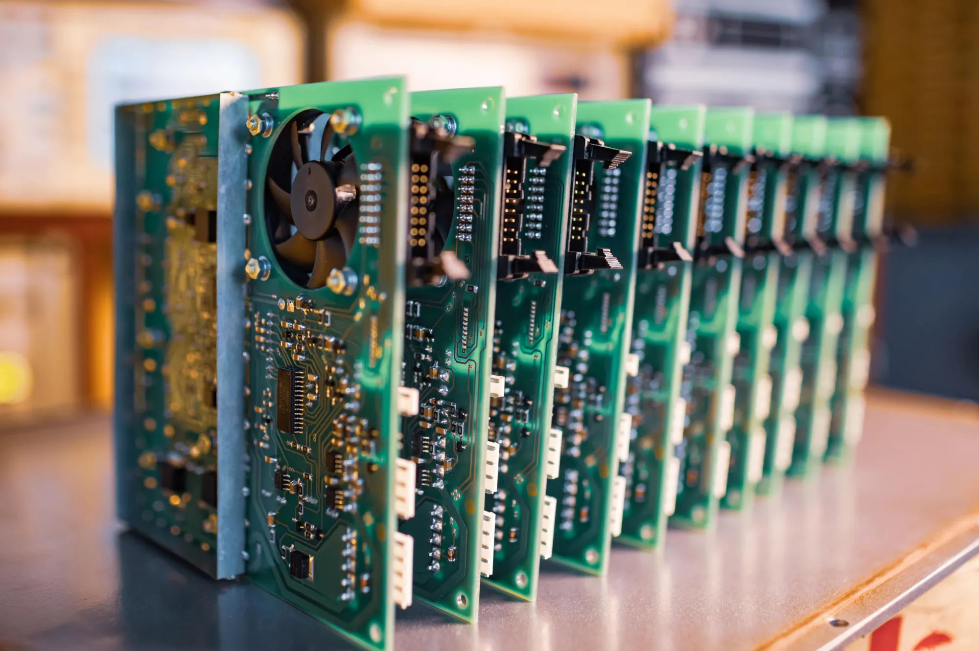
Board segregation, alternatively referred to as board partitioning, represents a strategic methodology for organising various circuit components within a Printed Circuit Board (PCB) to maintain their isolation. This approach significantly enhances the board’s performance, particularly concerning EMI reduction. This methodology not only mitigates electromagnetic interference but also optimises the signal integrity of the PCB design.
The core principles underlying these methodologies encompass:
- Managing the high-energy elements within high-frequency digital signals.
- Preventing common-impedance coupling amongst diverse circuit types within the board.
- Minimising current loop areas to reduce emissions and strengthen resistance to external interference.
High-Speed vs. Low-Speed Signals and Their Harmonics
The primary concept addresses the management of high-energy harmonic content generated by rapidly switching signals and their rate of current variation over time. Higher rates of current variation produce increased harmonic energy within signals, thereby elevating radiation probability.
The secondary concept relates to how signal frequency influences return current behaviour. This occurs because signal propagation impedance comprises not only conductor resistance but also capacitance and, crucially, loop inductance. The inductive impedance component increases proportionally with signal frequency.
Differences in Return Paths
Understanding that current invariably follows the path of least impedance is crucial. At higher signal frequencies, return current closely tracks signal current to minimise inductive loops. Conversely, at lower signal frequencies, where inductance becomes negligible, the resistive impedance component dominates.
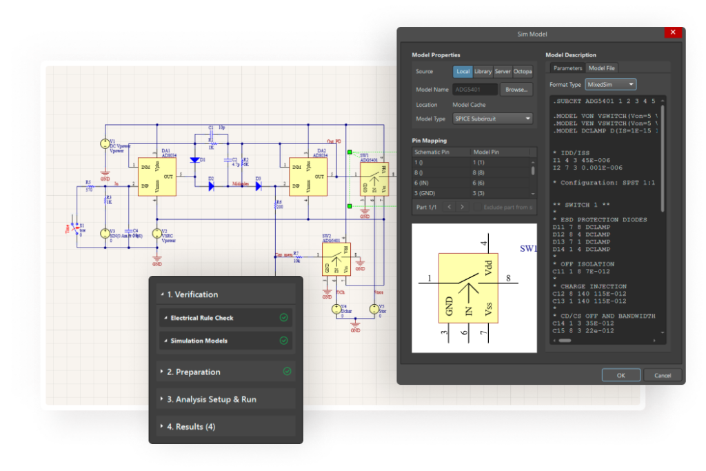
SPICE: Certainty for All Decisions
Design, validate, and verify the most sophisticated schematics. Learn More.
At this juncture, return current disperses across the conductor’s surface, seeking minimal resistance pathways. The critical consideration for PCB designers lies in understanding how signal frequency determines the return current’s path to its source.
As PCB design specialists, our primary objective is to minimise interference between these return currents, thereby preventing common-impedance coupling that could trigger electromagnetic emissions. We achieve this by establishing dedicated zones or sections within the PCB, each allocated to specific circuit types. This approach additionally reduces current loops, consequently diminishing radiation from differential-mode currents.
Whilst it may appear advantageous to implement a split in the Return Reference Plane (RRP) to enhance isolation between different circuit return current paths, this approach contradicts established EMC best practices. Such splits generate potential differences between metallic regions, effectively creating antenna-like structures that can amplify electromagnetic emissions in PCB design.
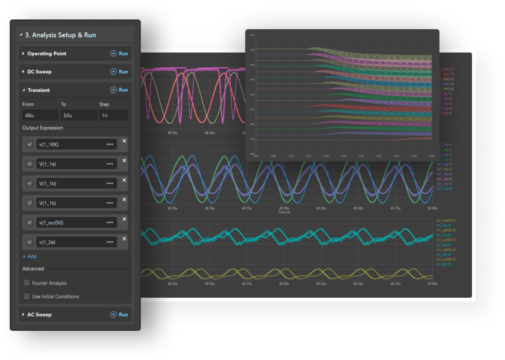
Easy, Powerful, Modern
The industry’s premier PCB design ecosystem. Explore Solutions.
The optimal approach involves implementing a continuous, low-impedance return reference plane that facilitates natural return current pathways to their sources. This plane must maintain integrity without cuts, splits, or substantial gaps that could generate common-mode noise. Component placement should be strategically organised into distinct zones based on circuit functionality and type.
For mixed-signal PCBs, the recommended segregation typically comprises distinct zones: digital, power, analogue, input/output, and when required, filtering sections. The digital section warrants particular attention and should maintain significant distance from other components. Despite return current following signal traces closely, the substantial harmonic energy content inherent in these signals presents increased radiation potential and coupling risks with other board sections.
A common manifestation occurs when clock signals couple with other networks across the board, particularly in power and analogue sections where connected cables may function as unintended antenna structures, promoting emissions.
Antenna Structures with Cables
The input/output section proves crucial for multiple reasons: limiting noise injection into cables, enabling isolation through filtering techniques, and implementing shielding to mitigate external interference and board emissions. The layout must account for cables and peripheral structures. Digital sections should maintain maximum separation from input/output areas, ideally positioned within the board’s interior, away from edges, preventing high-energy harmonic coupling to cables or edge radiation.

Furthermore, best practice dictates consolidating all input and output cables along a single board edge, rather than distributing them across multiple edges. This approach prevents potential differences between cables and minimises antenna-like structures that could propagate digital signals or noise.
Conclusion
Adherence to these guidelines significantly enhances your PCB’s electromagnetic performance, reducing radiated emissions whilst strengthening resistance to external interference.
Our subsequent article will delve into optimal PCB stackup selection strategies for enhanced EMI performance and reduced risk profiles. Stay connected through our platforms and social media channels for continued insights into advanced PCB design methodologies.
Delivering superior PCB design outcomes demands sophisticated tools that enable precise control across all design parameters. Our comprehensive PCB design ecosystem incorporates advanced layout capabilities, simulation features, and robust design validation tools, streamlining the board partitioning process whilst ensuring compliance with stringent requirements.
The sophisticated design rules engine and real-time simulation capabilities continuously verify adherence to specifications during PCB routing, maintaining exemplary design standards. Our secure cloud-based collaboration platform facilitates seamless file transfer to manufacturers, enhancing project coordination and fostering efficient teamwork throughout the development lifecycle.