A successful PCB starts long before production. Every stage of the assembly process, from design validation and component sourcing to soldering and QA, affects reliability, cost, and time to market.
If you’re building high-performance electronics for aerospace, defence, medical, or industrial use, you need confidence in how your boards are assembled. Understanding the process helps you reduce rework, speed up delivery, and ensure every unit meets spec, from first prototype to final production.
What the PCB Assembly Process Involves
PCB assembly is the process of turning a fabricated board into a functioning electronic system. It involves mounting and soldering components, either surface-mount, through-hole, or both, in line with the design’s electrical and mechanical requirements.
Where fabrication creates the physical board structure, assembly integrates the active and passive components that give it purpose. This step is critical to performance, reliability, and compliance, especially in industries where failure isn’t an option.
The PCB Assembly Process: Step-by-Step Guide
1. Design Review and DFM Checks
Before assembly begins, engineers review the Gerber files, BOM, and assembly drawings to confirm the design is complete, accurate, and build-ready. Design for Manufacturability (DFM) checks catch issues like mismatched footprints, incorrect pad sizes, or thermal relief problems, all of which can cause hefty delays or board failures downstream.
2. Component Procurement
Once the design is approved, components are sourced based on the BOM. This stage goes beyond availability; it involves matching specifications, packaging types, and confirming whether leaded or lead-free solder is required for compliance. Early procurement planning helps avoid last-minute substitutions and ensures compatibility with the assembly process.
3. Solder Paste Application
For surface-mount assemblies, solder paste is applied to each pad using a stencil. This step needs tight control because too much or too little paste can cause bridging, tombstoning, or poor joints. Precision here sets the foundation for both electrical performance and mechanical stability.
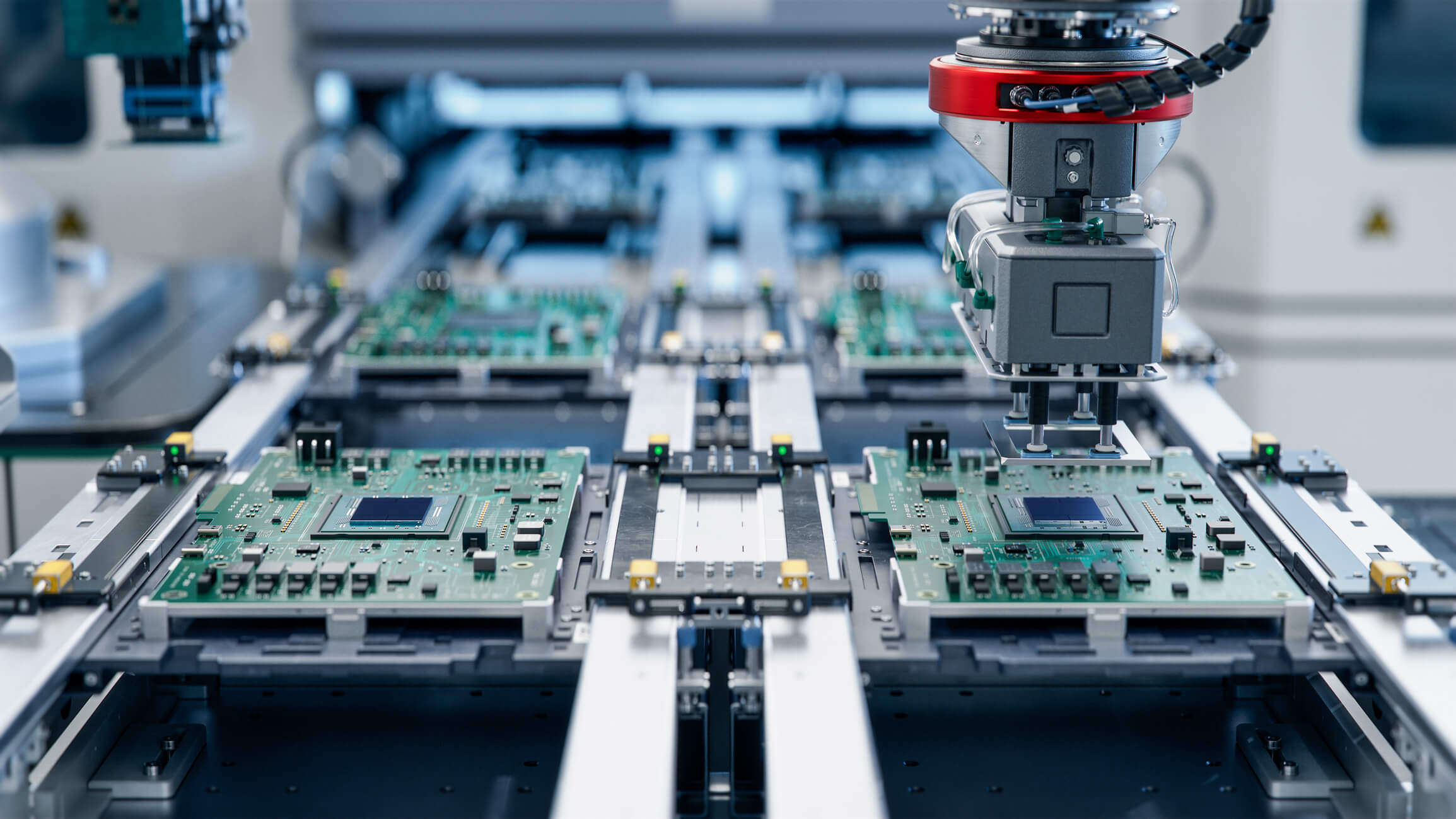
4. Pick and Place Assembly
Automated machines place components onto the pasted board with high speed and accuracy. This includes everything from passives to fine-pitch ICs, QFNs, and BGAs. Proper orientation, spacing, and alignment are critical, especially for high-density or mission-critical assemblies, where rework may not be possible once reflowed.
5. Reflow Soldering
The placed board then moves through a reflow oven, where temperature profiles are tuned to melt the solder paste and secure each component. Incorrect reflow settings can lead to cold joints, component warping, or incomplete bonds. For complex assemblies, multiple zones and controlled ramp rates will ensure thermal reliability.
6. Through-Hole Component Insertion
If your design includes connectors, high-current parts, or components that need mechanical strength, through-hole components are added next. These are typically soldered using wave or selective soldering. The process must be tuned to avoid overheating adjacent SMT parts or damaging multi-layer boards.
7. Conformal Coating or Encapsulation (If Required)
Boards intended for harsh environments, including defence, aerospace, and industrial use, may need added protection. Conformal coating will shield against moisture, dust, and vibration, but it must be compatible with the board material and not interfere with test points or connectors.
8. Inspection and Testing
Before delivery, every board must be inspected and tested. This may include AOI for SMT parts, X-ray for BGAs, flying probe or bed-of-nails testing, and final functional checks. For IPC Class 2 or Class 3 applications, inspection criteria are stricter, and traceability is often required. These measures ensure that the final product performs reliably under real-world conditions.
Scaling the PCB Assembly Process: From Development to Delivery
A reliable assembly process should support every stage of your product’s lifecycle — not just the first working board.
During prototyping, speed and flexibility are essential. With low-volume builds and evolving designs, this phase is about testing layouts, checking fit and function, and identifying potential issues early.
Quick turnaround times and adaptable sourcing help keep development on track while the design continues to evolve.
As the product moves closer to production, the focus shifts to consistency, control, and compliance. Reflow profiles are locked in, QA procedures are formalised, and every board must meet the same specifications across batches.
In regulated sectors, this often includes IPC Class 2 or Class 3 standards, process validation, and full traceability, all of which become critical as volumes increase.
At Masters & Young, we support this transition through tightly controlled in-house workflows and detailed documentation, ensuring your boards are built to spec, ready for the field, and consistent from the first unit to the thousandth.
Key Factors Behind a Reliable PCB Assembly Process
A smooth project starts with clean inputs. That means complete Gerber data, an accurate BOM, and clear assembly drawings. Any missing or inconsistent information can lead to misbuilds, delays, or costly rework, especially in dense or regulated designs.
Early DFM input helps prevent common issues before they reach the floor. Things like pad sizing, thermal relief, and component spacing all affect soldering quality and yield. Catching them early saves time and avoids production hold-ups.
Component sourcing also plays a critical role. It’s not just about stock. The right packaging type, leaded or lead-free compatibility, and part lifecycle status all impact the success of the build. Poor substitutions can introduce failures or derail compliance.
Open communication also keeps things aligned. Regular updates, well-documented changes, and clear escalation paths reduce the chance of missteps and help keep the project on track.
Quick-Glance Checklist: What You Should Have in Place
- Design files are build-ready: including Gerbers, BOM, centroid (pick-and-place) data, and assembly drawings
- DFM feedback has been reviewed and applied: covering pad geometry, thermal relief, spacing, and orientation
- Components confirmed and sourced correctly: matched to footprints, available for SMT or THT, and compliant with part lifecycle status
- Solder strategy defined: leaded or lead-free selected, thermal profiles optimised for complexity and density
- Version control locked: single source of truth for design revisions, build files, and BOM at all times
- Project communication protocols established: clear channels and regular check-ins to manage design or process changes
Experience A Stress-Free PCB Assembly Process with the Right Partner
A clear, controlled PCB assembly process makes the difference between delays and delivery. Whether you’re building aerospace systems, medical devices, or industrial electronics, the goal is always boards that work reliably, pass inspection, and perform under real-world conditions.
At Masters & Young, we focus on precision assembly, DFM insight, and in-house control, supporting your project from initial design through to production-ready delivery. We’re AS9100D and ISO 9001 certified, JOSCAR-registered, and DISP-listed, making us a trusted supplier for defence and aerospace applications.
With capabilities that span PCB design and manufacturing, SMT assembly, and full PCB assembly services, we help teams move faster, with fewer iterations and fewer surprises.
If you’re planning a new build or refining an existing design, contact us today and build with confidence from the start.