Printed Circuit Boards, or PCBs, are the foundation of almost every modern electronic device. They connect and support components such as resistors, chips, and connectors, allowing electricity to flow through precise pathways. Whether it’s a smartphone, a medical monitor, or defence equipment, each relies on a well-designed PCB to operate reliably.
In this guide, you’ll learn exactly what a PCB board is, how it works, and what it’s used for. We’ll keep the explanations clear and practical so you can understand both the basics and why PCB quality matters in professional manufacturing.
Quick Answer - What Is a PCB Board?
A PCB board, or Printed Circuit Board, connects and supports the electronic components inside a device. It uses copper tracks to carry signals and power between parts, replacing traditional wiring.
The main use of a PCB board is to make electronic systems reliable, compact, and easy to manufacture across industries like medical, defence, and consumer technology.
Understanding What a PCB Board Is
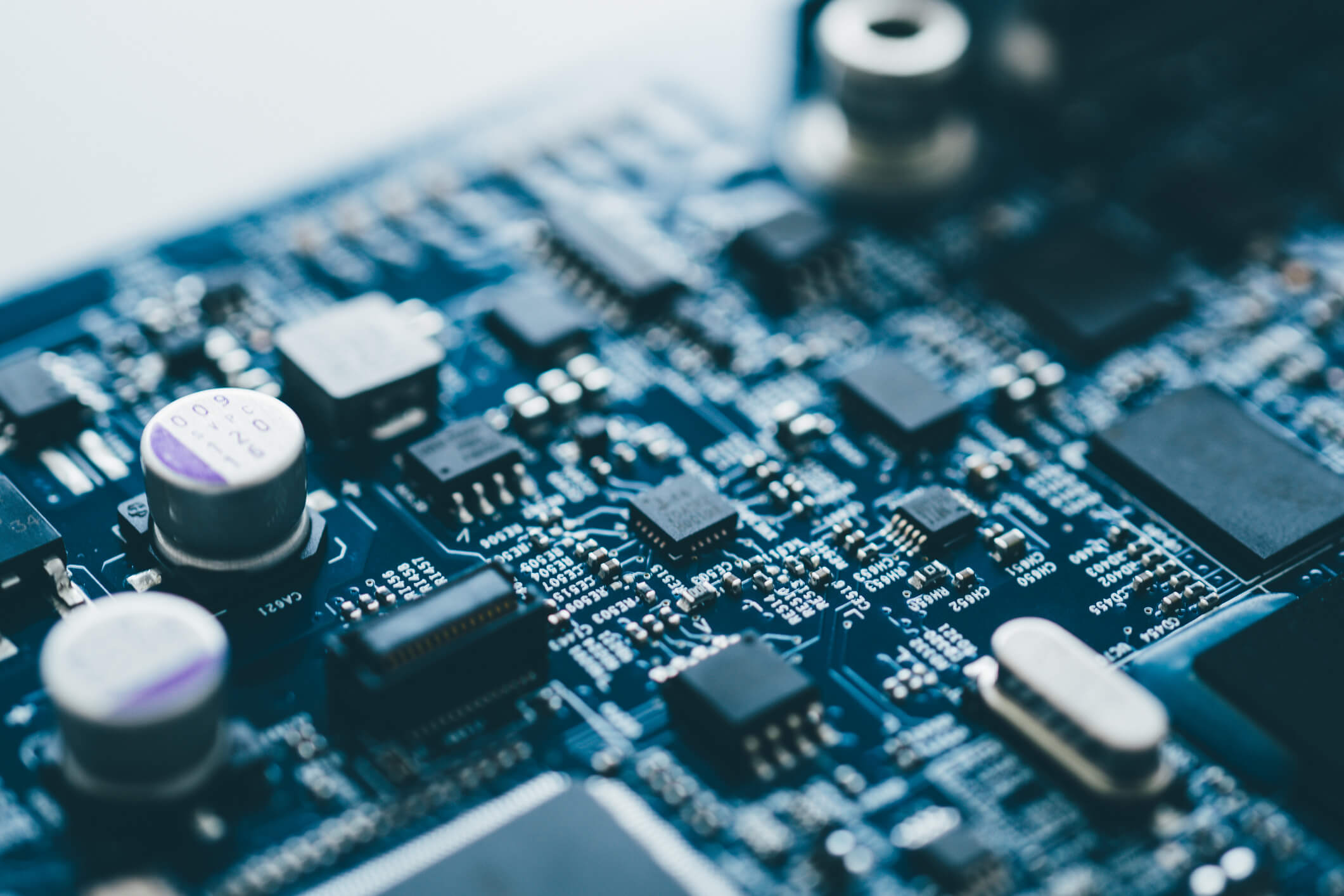
A Printed Circuit Board, or PCB, is the core platform that connects and holds electronic components inside a device. It provides both mechanical support and electrical connections, allowing current to move between parts in a precise and controlled way.
Most PCBs are made from an insulating material such as fibreglass, coated with thin layers of copper. The copper is etched into narrow pathways called traces, which form the circuit that links components together.
This design replaced older wiring methods that were bulky, unreliable, and hard to reproduce. Because a PCB can manage complex circuits in a small, consistent layout, it has become the foundation for everything from consumer electronics to medical and defence systems.
How a PCB Works
A PCB works by guiding electrical signals along copper tracks that connect each component on the board. These tracks act like roads, directing electricity to the right parts so the device can perform its functions.
Each board contains layers of conductive copper and non-conductive material. The copper layers carry electrical current, while the insulating layers prevent short circuits. Components such as resistors, capacitors, and integrated circuits are mounted on the board’s surface and linked through soldered connections.
When powered, the current flows through the traces, allowing signals to move between components at precise speeds and strengths. This controlled flow of electricity ensures the device operates safely and consistently.
By designing the circuit layout carefully, engineers can create boards that manage everything from simple lighting controls to more complex systems.
What Is the Use of PCB Board?
The main use of a PCB board is to connect and control electronic components within a device. It allows electricity to move accurately between parts, making electronic systems reliable, compact, and efficient.
PCB boards are used across almost every industry, including:
- Consumer electronics – smartphones, computers, TVs, and home appliances.
- Medical devices – patient monitors, imaging equipment, and diagnostic tools.
- Defence and aerospace – communication systems, control modules, and radar technology.
- Industrial systems – automation, robotics, and sensor control units.
By replacing complex wiring with precise copper pathways, PCBs make it possible to build advanced equipment that performs consistently under pressure.
In high-stakes applications, this reliability is critical, which is why Masters & Young is dedicated to designing and manufacturing boards that meet strict Australian and international standards.
Types of PCB Boards
PCB boards are built in different ways to meet specific electrical and mechanical needs. The main variations depend on how many conductive layers they have and how signals move across the board.
Common Types
- Single-Sided PCB: One copper layer for simple, low-cost circuits.
- Double-Sided PCB: Copper on both sides allows more complex connections, ideal for industrial controls and automotive systems.
- Multi-Layer PCB: Multiple copper and insulation layers stacked together to create compact, high-performance designs.
- Rigid PCB: Made from solid materials like fibreglass for stability and durability.
- Flexible PCB: Built from bendable materials such as polyimide, allowing the board to fold or twist without damage.
Advanced Types
- HDI PCB (High-Density Interconnect): Supports finer traces and smaller components for compact, high-speed electronics.
- High-Speed PCB: Designed for precise impedance control and rapid signal transmission, used in communication and defence systems.
These board types give engineers flexibility to balance performance, size, and reliability across industries such as medical, defence, and industrial manufacturing.
PCB Board Components and Materials
Every PCB board is made up of several layers that work together to deliver power and communication between components. Each layer has a specific purpose, and the quality of these materials determines how reliable and durable the board will be.
Main Layers
- Substrate: The base of the PCB, usually made from fibreglass or epoxy resin. It provides strength and insulation.
- Copper Layer: A thin sheet of copper that forms the electrical paths or “traces.” Some boards have one copper layer, while others have several.
- Solder Mask: The protective green (or sometimes other coloured) coating that prevents short circuits and protects copper from oxidation.
- Silkscreen: The top layer with printed labels, symbols, or markings to identify parts and connection points.
Common Materials
- FR-4: A durable fibreglass material used in most PCBs for its strength and heat resistance.
- Polyimide: Flexible and heat-tolerant, ideal for flexible PCBs.
- Aluminium: Used in boards that need better heat dissipation, such as LED lighting.
Masters & Young uses materials that meet AS9100D and IPC Class 3 standards, ensuring every board meets the strict quality demands of defence, medical, and industrial projects.
How PCB Boards Are Made
Making a PCB board is a precise and multi-stage process that turns a circuit design into a durable, high-performing electronic platform. Each stage must be carefully managed to ensure signal integrity, component accuracy, and long-term reliability.
1. Design and Layout
The process begins with electronic engineers creating the board layout using CAD software. This layout defines every component location, connection path, and layer configuration. Design tools also check for spacing, trace width, and electrical clearances to prevent short circuits.
At this stage, engineers decide on the number of layers, the board shape, and any mechanical features such as mounting holes or cut-outs. Careful design ensures the finished board performs as expected in its final application.
2. Fabrication
Once the design is finalised, the fabrication process begins. The copper-clad laminate is cleaned and coated with a light-sensitive film. The circuit pattern is transferred onto the copper using ultraviolet light, and the unwanted copper is etched away to reveal the tracks.
For multi-layer PCBs, individual layers are created first and then laminated together under heat and pressure. Holes known as vias are drilled to connect copper layers vertically. The holes are then plated to form reliable conductive paths between layers.
3. Surface Preparation and Solder Mask Application
The surface of the board is cleaned to remove oxidation or debris. A solder mask is applied next, forming the familiar green protective coating. This layer prevents accidental solder bridges between traces and protects the copper from corrosion.
4. Silkscreen Printing
The silkscreen layer adds component labels, polarity markings, and reference indicators. It helps technicians identify where each component belongs during assembly and simplifies future inspection or maintenance.
5. Assembly and Component Placement
During assembly, electronic components are mounted on the board using Surface Mount Technology (SMT) or Through-Hole Technology (THT).
- SMT places small components directly onto copper pads, allowing for compact layouts and automated production.
- THT inserts component leads through drilled holes and solders them from the opposite side, often used for larger or high-stress parts.
Automated pick-and-place machines position each component with precision measured in fractions of a millimetre.
6. Soldering
After placement, the board goes through soldering. In reflow soldering, heat melts solder paste applied earlier, bonding each SMT component in place. In wave soldering, molten solder flows under the board, connecting THT components quickly and evenly.
7. Testing and Quality Assurance
Every PCB undergoes multiple inspections to confirm its reliability before delivery.
- Automated Optical Inspection (AOI) checks for missing parts, misalignments, or solder defects.
- Flying Probe Testing measures electrical continuity and verifies correct connections between points.
- Visual inspections and functional tests ensure the board meets both design and performance specifications.
At Masters & Young, all boards are built under an AS9100D-certified quality system and inspected to IPC Class 3 standards, which is the highest level of electronic workmanship.
This guarantees that each PCB performs under demanding conditions, from aerospace missions to medical and defence applications.
Start Your PCB Project with Masters & Young
Every reliable electronic device begins with a well-designed PCB. Whether you need a simple prototype or a complex multi-layer board built to defence standards, Masters & Young can help you turn your concept into a working solution.
Our Brisbane-based team handles the entire process, from design and layout to manufacturing, assembly, and quality assurance, all under AS9100D and IPC Class 3 standards.
We focus on precision, performance, and long-term reliability across defence, aerospace, medical, and industrial applications.
If you’re ready to begin your next project, we’re ready to support you. Contact Masters & Young today to start your PCB process with an experienced Australian team that delivers quality from start to finish.
FAQs
What is the difference between PCB and PCBA?
A PCB (Printed Circuit Board) is the bare board that connects components through copper tracks. A PCBA (Printed Circuit Board Assembly) is the finished product after all components have been mounted and soldered.
Can a PCB board be repaired?
Yes, a PCB can often be repaired if the damage is limited. Broken traces can be bridged, and faulty components can be replaced. However, repairs should be done by skilled technicians using proper tools to avoid further damage.
How many layers can a PCB have?
PCBs can range from a single layer to more than 20 layers, depending on the design complexity. Multi-layer boards are common in advanced systems such as communication, defence, and computing equipment.
What determines the quality of a PCB?
Quality depends on material selection, precision in copper etching, clean soldering, and thorough testing. Boards built under certified systems like AS9100D and IPC Class 3 provide consistent performance and reliability.
Why are most PCBs green?
The green colour comes from the solder mask, a protective layer that shields copper from corrosion. Green has become standard because it provides high contrast for visual inspection, but other colours like blue, red, or black are also used.
What industries use high-performance PCBs?
Sectors such as defence, aerospace, medical, and industrial automation rely on high-performance PCBs. These boards must meet strict environmental, mechanical, and safety standards to operate in critical conditions.